

Pat Gelsinger is familiar with the graveyard of failed memory technologies. “We haven’t had a new memory for three decades,” says the former Intel CEO. SRAM, DRAM, and flash memory still dominate. Gelsinger has witnessed the rise and fall of several potential alternatives—most recently Optane, Intel’s failed attempt to create “universal memory.”
But Gelsinger, who is now a general partner at venture capital firm Playground, believes that AI is forcing a rethink of the entire computing stack—and that memory is a key part of that shift.
Playground has backed Nagare Labs, a company spun out of Georgia Tech working on a prototype memory technology called Z2RAM. Instead of replacing existing memory, Z2RAM will attempt to offer a new layer in the existing memory stack that could prove useful for AI workloads and for other tasks that benefit from low latencies.
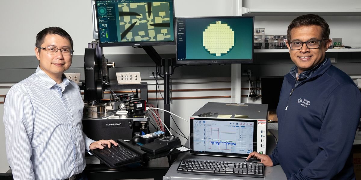
“This is an SRAM addition, rather than a DRAM replacement,” says Suman Datta, a Georgia Tech professor and former Intel transistor researcher. Datta cofounded Nagare Labs with colleague Shimeng Yu. The company emerged from stealth on 26 October with US $5 million in funding led by Playground.
Z2RAM for Faster Memory
Datta says Z2RAM’s name also describes its design. “Z2” refers to two Zs: The first stands for stacking in the z (vertical) axis; the second stands for zero capacitor.
A conventional DRAM cell stores a bit as charge on a capacitor. Reading the bit drains it, so the data must be written back each time. That stretches DRAM access to 40 to 50 nanoseconds, Datta says.
Z2RAM ditches the capacitor and uses two transistors per cell instead. The first writes the bit and the second reads it without disturbing it, so the two operations no longer share a port as they do in DRAM, where every read drains the capacitor and causes a write-back. Putting the charge on the read transistor’s gate also amplifies the signal, so a smaller stored charge can still be sensed quickly.
Datta says this new design yields best-case estimated read speeds of one to two nanoseconds, making Z2RAM significantly faster than DRAM. And although it’s still not quite as fast as SRAM, it has the potential for much greater density. An SRAM cell is built in the same front-end design process as the processor it’s a part of, so every additional bit competes for area on an expensive logic die. In addition, the size of an SRAM cell has proven increasingly difficult to shrink.
Nagare’s solution is to stack the bits. The company’s first generation of Z2RAM will target six layers, for a target density of 185 megabits per square millimeter. Datta says that’s about five times what SRAM achieves. Eventually he projects that the company could stack up to 106 layers, which, if it proves possible, would give Z2RAM a density 90 times as great as SRAM.
Datta says stacking is possible because Z2RAM’s transistors can be built with plasma-enhanced atomic layer deposition at less than 450 degrees Celsius. Although hot, it’s still relatively cool enough to add memory layers on top of a finished CMOS wafer without degrading it. Nagare’s plan is to tape out the memory’s control circuits first on a mature logic process, then build the memory array above, with multiple layers per lithography step. The finished chip can then be bonded on top of a processor as a chiplet.
Overcoming Z2RAM Memory Stability Hurdles
Z2RAM’s goals still face notable technological hurdles. Datta says that when a write ends and the write transistor switches off, capacitive coupling from its control line disturbs the stored charge, which narrows the margin for reading the bit and could lead to read errors.
Nagare Labs’ answer is a patented metal shield inside each cell, which separates transistors. Using a shield is not without its downsides, as it makes each cell physically wider, which in turn reduces the memory’s density. Z2RAM expects vertical stacking to mitigate the issue.
Stability is another potential obstacle. “Right now the biggest challenge for oxide semiconductor transistors is the threshold voltage stability under bias and temperature stress,” Datta says. If the voltage at which a transistor turns on drifts, a stored bit can be misread. Fixing that issue requires tuning the channel, the gate stack, and the contacts together. Nagare is still experimenting with various recipes that use oxides of indium and gallium, sometimes with zinc added, as well as with tungsten-doped indium oxide, to find the best solution.
Making the connection between Z2RAM and a processor is the final hurdle, as there’s no standard for how this new kind of memory attaches to an AI chip. Datta sees an opening provided by high-bandwidth memory, where the industry is shifting from standard designs toward custom ones. Memory designs typically conform to standards by JEDEC, an industry standards organization, but companies looking for memory to pair with AI accelerators are more amenable to a customized solution.
Z2RAM for Edge AI and Robotics Latency
For Gelsinger, the next milestones are clear: Get the device out of a university lab, sign a fabrication partner, and demonstrate it on standard 300-millimeter wafers. He says the $5 million provided by Playground is only the start of what Nagare Labs will require to complete its work. “This will be multiple tranches of real funding,” he says. Datta agrees. “This company requires a lot of runway, both in terms of capital and time,” he says.
In addition to AI accelerators in data centers—a market that all memory technologies currently have in their crosshairs—Datta sees an opportunity in edge AI for robotics. He notes that robots may use a vision model that doesn’t require much memory capacity but that requires extremely low latencies to provide a real-time understanding of the environment. Such systems could be a good fit for Z2RAM.
For now, though, Datta is focused on the tricky path from R&D to Z2RAM’s first commercial memory chips, which could still be years away. “I always tell my students that the application will emerge just based on the capability of your technology,” he says.
From Your Site Articles
Related Articles Around the Web
